The automotive industry is undergoing a revolution unlike any other time in its history. The proliferation of sensors such as cameras, LiDAR, and radar in automobiles has led to the emergence of advanced driver-assistance systems (ADAS) which are equipping modern vehicles with unprecedented functionality in terms of autonomy, safety, and performance.
However, with the increase in sensor activity, the industry is also seeing significant challenges on the hardware, compute, and design sides. Specifically, the amount of data being produced by these sensors is creating issues in terms of data management, control, and processing. At the same time, achieving performance and safety requires real-time, low-latency processing of this data.
All of these factors has led to the realization that general-purpose computing hardware is no longer up to the task. To achieve the highest levels of vehicle autonomy, the industry has shifted to hardware acceleration and custom electronics in place of off-the-shelf components. While ASICs provide the highest performance and lowest power consumption, they do not allow for any flexibility if the design requirements change. Moreover, ASICs suffer from long development cycles compared to FPGA-based solutions.
In today’s fast and dynamic world, the industry needs hardware that can not only support acceleration but is also flexible enough to keep up with changing algorithms and sensor technology. This required flexibility can be achieved through the combination of ASICs/SoCs with embedded FPGA (eFPGA) technology — a solution uniquely poised to enable the future of ADAS.

Achronix Solutions
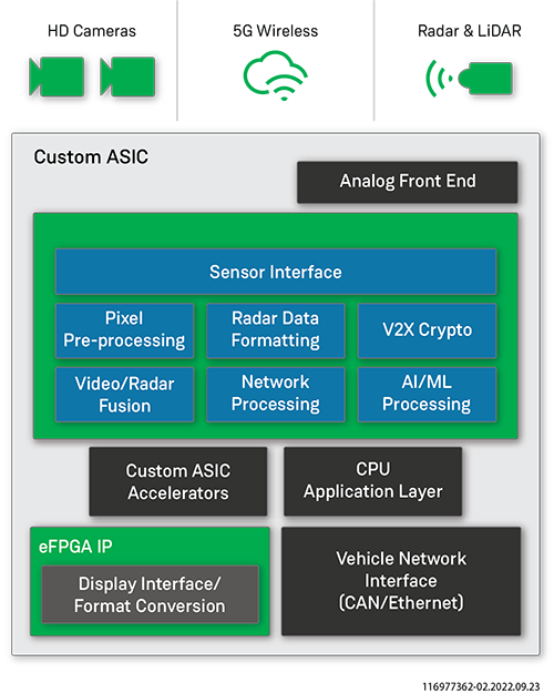
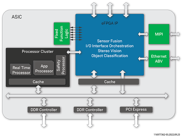
When it comes to designing hardware for ADAS, the challenge lies in supporting the extensive number of applications and interfaces required. From a high level, an ADAS compute engine will first rely heavily on its sensor interface. Equipped with multiple high-throughput sensors, modern-day vehicles require computing hardware that can quickly and reliably interpret, manage, and control the flow of data through processes known as sensor fusion. From a hardware perspective, sensor fusion requires compute blocks with ultra-high bandwidth connectivity to both external high-speed interfaces as well as data routing within the device.

A Custom SoC to Support the Plethora of ADAS Applications
Second to sensor fusion, communications as a whole are a crucial aspect of ADAS. Vehicle network interfaces for protocols such as CAN and Ethernet, as well as support for wireless communication standards such as 5G, impose unique computing requirements on the system.
Looking beyond communications, the application-specific tasks required can be extremely varied. From a driving-performance perspective, a single ADAS solution often relies on a number of unique tasks, such as pixel pre-processing, data formatting, and AI/ML processing. From a security perspective, cryptographic engines are also a must for ADAS as sensitive user data may be compromised through vehicle-to-everything (V2X) connectivity. Finally, user experience (UX) is a crucial element of ADAS, where display interfacing and format conversion are necessary processes in providing an infotainment display that creates a natural and intuitive user experience with an ADAS implementation.
Each of these tasks is equally as crucial to the overall performance of an ADAS implementation, but each also features unique computing requirements that do not always overlap with one another. To support these varying requirements, system architects often develop proprietary SoCs, allowing multiple dedicated hardware blocks to be optimized for each given application, ensuring high performance overall.
eFPGA Benefits
One of the defining features of ADAS is the need for fast processing to enable near real-time decision-making — decisions that could mean the difference between life and death for the vehicle's occupants. For this reason, the underlying compute in ADAS implementations requires extremely powerful processing capabilities with the lowest latency possible. At the same time, when looking at electric vehicles (EVs), designers also encounter strict requirements for low-power processing to extend the vehicle battery life as far as possible. This unique combination of low-latency, low-power processing makes ADAS a particularly challenging field.
Fortunately, FPGAs are particularly well suited to meet these requirements, making them ideal hardware accelerators, offloading the compute-intensive machine learning algorithms that ADAS relies on. Out of this comes an improvement in both processing speed and power expenditure as compared to CPU and GPU-based systems. The latter is where FPGAs really shine, as FPGAs offer better performance per watt than the alternatives.
The value of FPGAs in automotive design has long been established as the technology has been used in over 200 million vehicles over the last 15 years. However, looking beyond the FPGA, it is clear that, for the needs of ADAS today, the eFPGA reigns supreme.

eFPGAs as Compared to Discrete FPGA Solutions
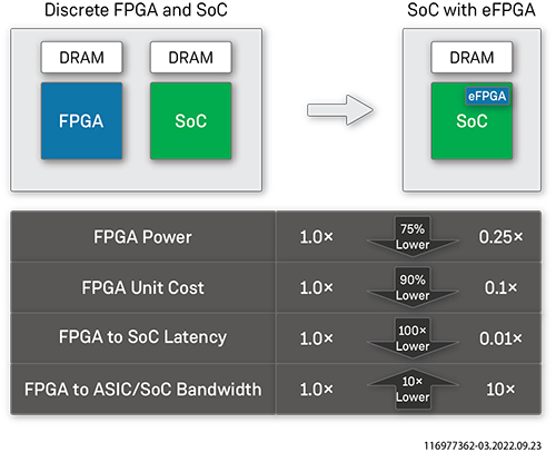
The real value proposition of eFPGA IP in ADAS applications versus standalone FPGAs is its ability to be integrated within an SoC, sized to the team's exact resource requirements. An eFPGA instance adds flexibility while lowering system cost, power and board space by eliminating the excess features of the standalone FPGA which are not required when moving into high-volume production. Moreover, integrating eFPGA IP enables designers to achieve a tight coupling of an FPGA fabric with other SoC resources such as an embedded CPU or specialized interfaces. It is this tight coupling and the elimination of power-hungry I/O that enable eFPGAs to deliver unprecedented performance and power savings versus using a standalone FPGA as a sidecar to an SoC.
Embedding an eFPGA instance in an SoC offers other important advantages such as the ability to update algorithms in the field through OTA software updates. Moreover, eFPGAs help reduce the BOM, where, as compared to a standalone FPGA solution, an eFPGA is likely to provide ADAS designers 80%-90% lower overall system cost.
Achronix Products for ADAS
Achronix Speedcore eFPGA IP offers a unique architecture that incorporates many features which can increase performance, reduce power consumption, and reduce die area. When specifying a Speedcore eFPGA instance, designers can select the optimal mix of architectural elements including:
- Logic – 6-input look-up-tables (LUTs) plus integrated wide MUX functions and fast adders
- Logic RAM – 2 kb per memory block for LRAM2k, and 4 kb per memory block for LRAM4k
- Block RAM – 72 kb per memory block for BRAM72k, and 20 kb per memory block for BRAM20k
- DSP64 – 18 × 27 multiplier, 64-bit accumulator, and 27-bit pre-adder per block
- Machine learning processors (MLP) – 32 multiplier/accumulators (MACs) per block, supporting integer and floating point formats

A Speedcore-based ADAS SoC
In most situations, automotive designers need to produce their SoCs at scale to support the large quantities of vehicles to be sold on a yearly basis. Speedcore eFPGA is one of the only embeddable fabrics on the market today that is production proven in large quantities — to date, our customers have successfully shipped over 15 million devices that incorporate our Speedcore technology.
Beyond the ability to support high-volume production, our Speedcore IP is bolstered by the comprehensive set of tools and offerings that we offer. For designers, we have leveraged our experience shipping standalone FPGAs in developing our Achronix Tool Suite. The suite itself comes with the Achronix proprietary ACE design tools as well as Synplify-Pro synthesis from Synopsys. Other tool offerings include Snapshot Debugger, a real-time design debugging tool as well as a number of Achronix-specific simulation libraries. Altogether, the Achronix Tool Suite is the culmination of over 15 years of tool development and improvement.
Combining silicon-proven tools with production-proven eFPGA IP results in a power solution for ADAS designers.
Learn More about Achronix in ADAS Applications
To learn more about how FPGA and eFPGA IP can enable unprecedented performance in ADAS, visit:
- How to Meet Power Performance and Cost for Autonomous Vehicle Systems using Speedcore eFPGAs
- Embedded FPGAs for Next-Generation Automotive ASICs
- How to Meet Self-Driving Automotive Design Goals Part 1
- How to Meet Self-Driving Automotive Design Goals Part 2
- eFPGA IP Workload Acceleration for Autonomous Vehicles | Achronix Webinar
